Importance of Silkscreens for PCB Identification and Labeling
Just as the signal lights of your car help to indicate when your car plans to take a turn or change lanes, the silkscreen is also used in the PCB process to help in testing and troubleshooting the board. The layer of silkscreen contains information regarding the PCB assembly process. This includes the location of components, their polarity and details for their placement and orientation, identifiers, labels and logos for various components. Your silkscreen must have a clear and readable font. In order to explain why silkscreen is so crucial let us discuss its importance in assembly and testing of PCBs.
Importance of Silkscreen in PCB Assembly
In the past, silkscreen was applies by using a stencil to directly apply ink into the boards surface. In the present time we use LPI (Liquid Photo Imaging) and DLP (Direct Legend Printing) instead.
LPI gives higher resolution of images and text, although it is time-consuming. The process involves exposing an imageable film to UV light (quite similar to the method used in applying solder mask).
DLP on the other hand, is not time-consuming. In this case an inkjet printer is used to print the silkscreen on the board with the help of acrylic ink.
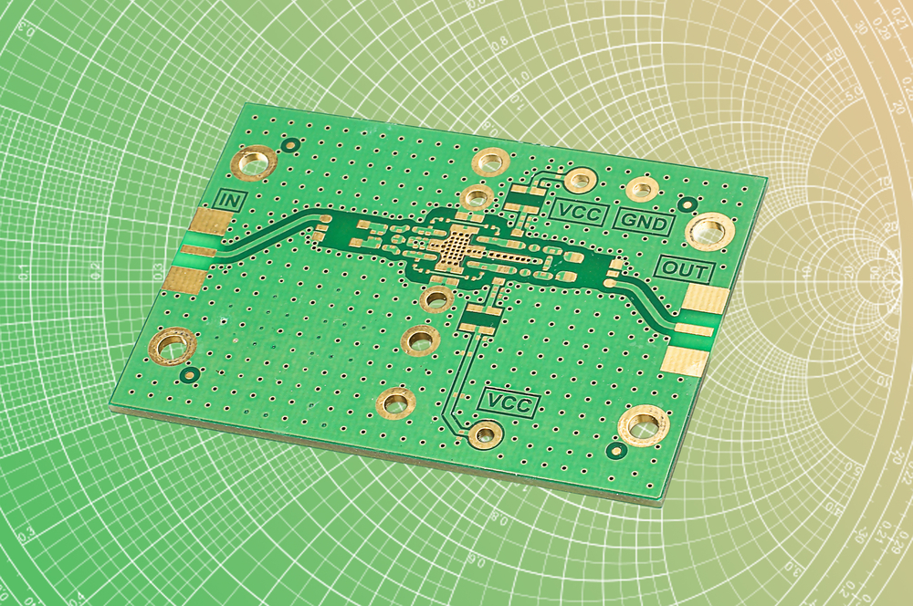
The silkscreen is used then in the PCB assembly process, particularly in the placement of components. The silkscreen markers help to give accuracy to the placement process. The silkscreen markings may include:
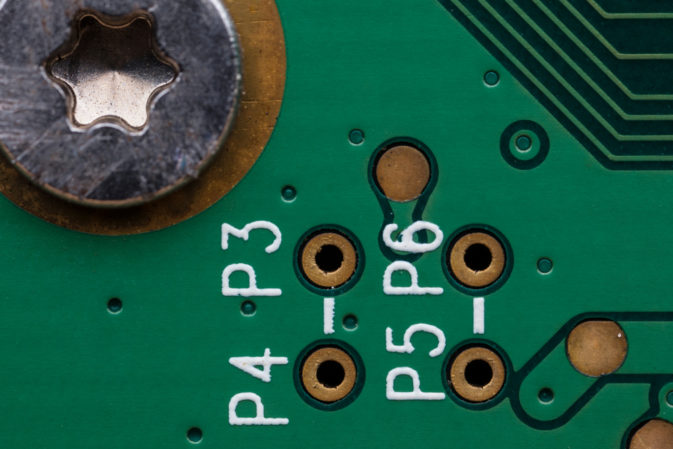
Reference Indicators: They help to identify component types from the ‘Bill of Materials’ (BOM)
Pin 1 Indicator: They indicate which pins connect to what pads of the footprint
Polarity Indicators: They help indicate the orientation of polarized components.
Component Outline: This helps indicate where the components are to be placed.
For simpler components with a small number of pads, the component outline is not essential, but will be required for general placement. Whereas, reference indicators, pin 1 and polarity indicators are important and cannot be missed or you may end up with misplaced components.
Importance of Silkscreen in PCB Testing
PCB silkscreen is also used in providing the engineer/technician with the location where measurements are to be taken during the testing and troubleshooting process. This can help in identification of potential failure causes, and verification of device performance. Some silkscreen markings used for testing/troubleshooting include:
Test points: They are used to indicate locations on the board where desired values are known. This is useful for identifying problems with board operation.
Warning Symbols: They help indicate parameters that should be avoided or handled with care such as high voltage points.
Part Numbers: They are helpful in case of the absence of datasheet and helps provide device information.

Tips for Silkscreen PCB Design
Here are a few tips to help you make sure your silkscreen is accurate and can be used in testing and assembling of PCBs.
Use fonts approved by your CM. Some fonts may be easy to create in software but difficult to generate in board manufacturing.
Use black or white color as silkscreen so it is readable and is in contrast with your board soldermask.
Follow your CM’s clearance and dimensions guidelines, this ensures that your silkscreen is not covered by components.
Conclusion
Adding silkscreen to your PCB layout will help you assist others in your PCB manufacturing process and testing too. But it will only pay off if your silkscreen is readable and clear. To avoid issues later on you should give attention to your silkscreen requirements so your PCB may be as accurate as possible!

See More in Electronics: